


XC7A100T
Model
AC7100BTemperature class
-40℃~85℃Ean
6971390270981Price
$ 340Suitable for high-speed data communication, video image processing, high-speed data acquisition, etc
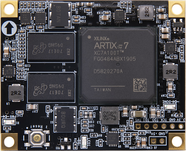
*Learn about the corresponding development board, click to view the details>>
*Learn about the corresponding development board, click to view the details>>
*Learn about the corresponding development board, click to view the details>>
Core Board
AC7100B
FPGA Chip
XC7A100T-2FGG484I
Speed Grades
-2
Chip level
Industrial grade,-40°c~85°c
RAM
1GB DDR3 , 32bit
QSPI FLASH
16MB
Logic cells
101440
Look Up Tables
15850
trigger
126800
Max.Distributed RAM
1188
Block RAM (36Kb each)
135
Total Block RAM
4860kb
DSP Slices
240
Transceiver
4x6.6Gbps
PIC Express
PCIE2.0
HR IO
180
Differential pair LVDS
48
Power Connector
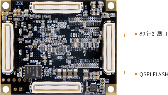
80pinx4
DDR3
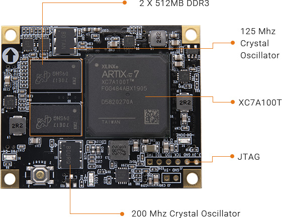
Two DDR3 chips are 1GB in total, each chip is 512MB, 32bit bus, and the data rate is 800Mbps
QSPI Flash
One 128Mbit QSPI flash, which can be used for FPGA user data storage
Crystal oscillator
The high-precision LVDS active differential crystal oscillator provides a stable clock source for the system at 200MHz and a stable clock input for GTP transceiver at 125MHz
transceiver
4-way GTP, each up to 6.6gb/s, suitable for optical fiber communication and PCIe data communication
working temperature
-40°c~85°c
PCIe 2.0
support PCI Express 2.0x4
Analog to digital conversion/XADC
1個12bit, 1Mbps AD
JTAG
Single row test holes with 2.54mm spacing of 6 pins
LEDs
1 LED
Voltage Input
+ 5V
FPGA Core Board
1 Piece
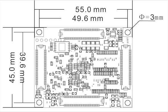
Size Dimension
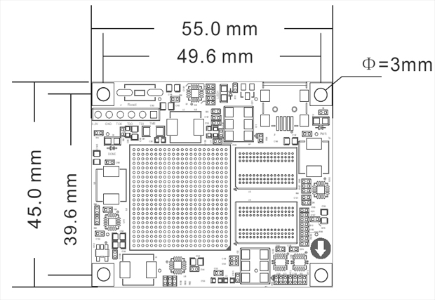
45mm*55mm*6.0mm
Connector Height
1.6mm
Connector Height
3.0mm
Number of Layers
10-Layer Core Board PCB
Super Combination with DDR3 Memory
6.6Gb/s, 4 x GTP , 1GB DDR3 RAM

Provide Schmatic, PCB, Structure Size, Package, Reference Design Convenient for secondary development

High-Speed Data Transmission, High Bandwidth and Capacity Apply to Data Acquisition and Communication, Video Image Processing

The warranty period of all products sold is 12 months, of which FPGA chips and LCD screens are wearing parts and are not covered by the warranty. All accessories and gifts are not covered under warranty.