

XCKU040
Model
AXKU042Ean
6971390271759Price
$ 1400For high-speed data transmission and exchange, pre-verification and post-application of data processing is possible

*For more information on the Core Board click >>

FPGA Chip
XCKU040-2FFVA1156I
Chip level
Industrial Grade
DDR4
4GB DDR4, 64bit
Logic Cells
530K
CLB LUTs
242,400
CLB Flip-Flops
484,800
Max. Distributed RAM (Kb)
7,050
Block RAM (36Kb each)
600
Total Block RAM
21.1Mb
DSP Slices
1920
transceiver
20 x 12.5Gbps
PCI Express
PCIE 3.0
HR IO
255
HP IO
99
LVDS
120
DDR4
4 x 1GB DDR4
QSPI Flash
Two 128Mbit QSPI flash memory chips can be used to store FPGA chip configuration files and user data
Optical fiber interface
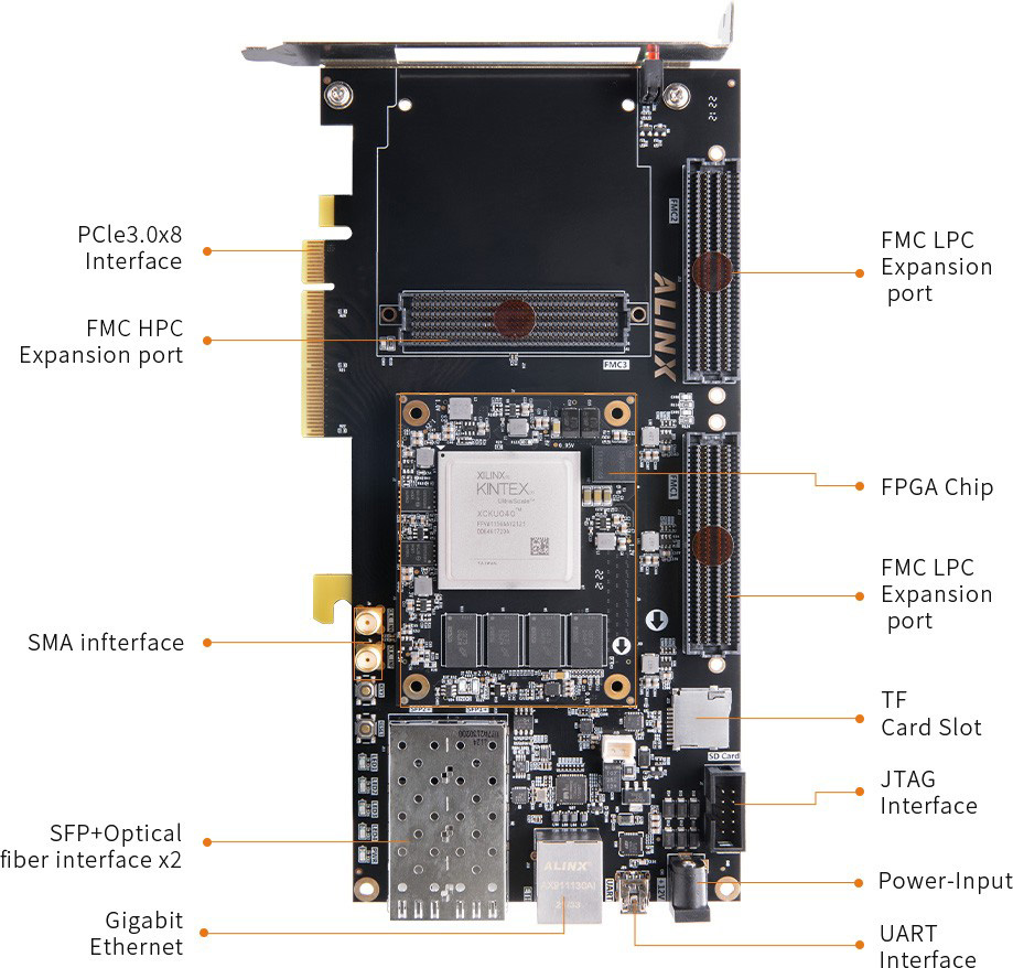
2-way SFP + optical fiber interface to realize 2-way high-speed optical fiber communication interface. The receiving and transmitting speed of each channel of optical fiber data communication is as high as 12.5Gb/s
FMC Extension interface
Three standard FMC expansion ports, including two LPC expansion ports and one HPC expansion port. External Xilinx or alinx FMC daughter boards (HDMI input and output module, binocular camera module, high-speed AD module, etc )
PCIE X 8 Interface
1-way PCIE3.0 X 8 interface for PCIE data communication with PCs
USB Uart
1 Uart to USB interface for communication with computer and user debugging
Ethernet interface
One 10/100m/1000m Ethernet RJ45 interface is used for Ethernet data exchange with computers or other network devices
SMA interface
2-way SMA External Interface for External High Speed Input and Output Signals
Crystal Oscillator
Two 156.25Mhz differential crystal oscillator, which gives the transceiver a reference clock
JTAG
10-pin 2.54mm standard JTAG port for downloading and debugging of field programmers
Temperature Sensor
Sensor Chip LM75A, Used to Detect the Ambient Temperature
EEPROM
One EEPROM for LC bus communication and storage of customer-defined information
SD Card Slot
1-way Micro SD card holder for data read, write and storage of SD card by GA
LEDs
1 power indicator; 4 user lights, 2 panel lights
KEYs
1 reset button, 1 normal IO connected to the GA
Voltage Input
+12 V DC
Current Input
Max. Current 3A
FPGA Board
1
DC Fan (Fixed on the Board)
1
Mini USB Cable
1
USB Downloader Cable
1 Set
12V Power Adapter
1
Size Dimension
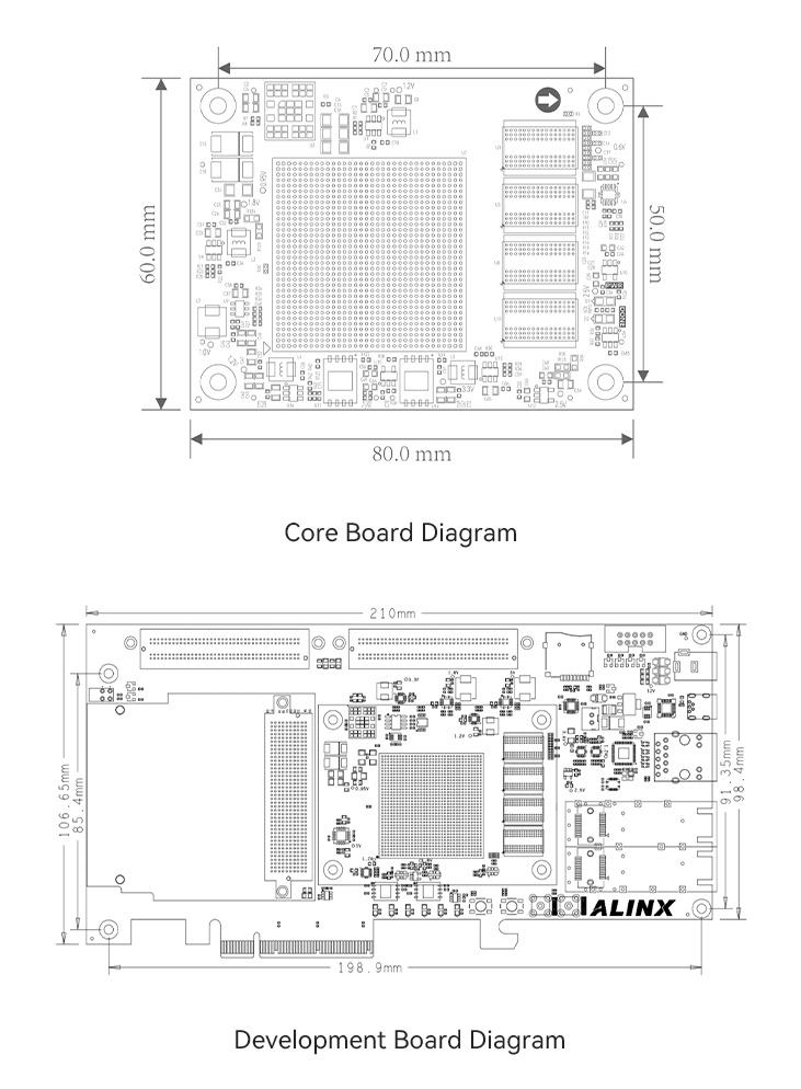
210mm x 106.65mm
Number of Layers
Core panel 18 PCB board design, extension panel 12 PCB board design, reserve separate power layer and GND layer

High speed optical fiber communication, video processing, high-speed data transmission processing, etc

Support the requirements of high-speed data transmission and exchange, data storage, video transmission processing and industrial control, and the verification in the early stage of project development
Rich peripheral interfaces: 2 × 10G SFP+optical interface, 3 FMC extension interfaces (1 HPC, 2 LPC), 1 Gigabit Network port, 1 UART serial port, 1 SD card interface, LED keys and so on

The warranty period of all products sold is 12 months, of which FPGA chips and LCD screens are wearing parts and are not covered by the warranty. All accessories and gifts are not covered under warranty.