

XC6SLX9
Model
AX309Price
$ 80
Xilinx Kintex UltraScale FMC HPC Optical fiber FPGA Development board XCKU040

Xilinx Artix7 SFP FPGA Development Board XC7A200T

Xilinx Zynq UltraScale+ MPSoC AI FPGA Development Evaluation Board XCZU2CG

Xilinx Zynq UltraScale+ MPSoC XCZU4EV FPGA Development Board

XILINX Zynq7000 SoC FPGA Development Board XC7Z010

Supporting routines and supporting materials development board All supporting materials are provided through Baidu Netdisk. After purchasing, please contact customer service to request
Basic Tutorial
01. ISE14.7 Software Installation
02. Downloader Driver Installation
03. Install Modelsim software and settings
04. Write testbench and simulation
05. ISE Engineering Modelsim Simulation Validation
06. Verilog Basic Module and Grammar Learning
Experimental routine
01. Experiment on LED Flowing Light under ISE14.7
02. ISE14.7 Button Down Experiment
03. PLL phase-locked loop output under ISE14.7
04. Serial port transceiver experiment
05. Digital tube scanning experiment
06. Button shake elimination experiment
07. PWM Buzzer Experiment
08. Buzzer plays music
09. SPI_ Flash Reading and Writing Experiment
10. Digital tube display RTC time experiment
11. I2C interface EEPROM experiment
12. FPGA on chip ROM read test
13. FPGA on-chip RAM read and write test
14. FPGA on chip FIFO read and write test
15. SD card reading and writing experiment
16. VGA color bar output
17. 4.3 inch screen color bar output
18. 7-inch screen color bar output
19. SDRAM Reading and Writing Test Experiment
20. AN831 Recording and Playback Routine
21. SD card&AN831 music playback
22. Character VGA display
23. Character 4.3 inch screen display
24. Character 7-inch screen display
25. SD card image VGA display
26. SD card image displayed on a 4.3 inch screen
27. SD card image displayed on a 7-inch screen
28. AN5640 camera captures VGA display
29. AN5640 monocular camera captures a 4.3 inch screen display
30. AN5640 monocular camera captures 7-inch screen display
31. Camera image color to black and white display
32. Camera SOBEL edge detection routine
33. AD9238 waveform display routine
34. AD7606 waveform display routine
35. ADDA waveform test VGA display
36. Snake Game Design
AN108 AD/DAPackage
AN9767 DA Package
AN706 AD Package
AN9238 AD Package
AN831 Package
Single camera video package
Luxury Package
Development Board
●
●
●
●
●
●
●
downloader
●
●
●
●
●
●
●
AN108
●
●
AN9767
●
●
AN706
●
●
AN9238
●
●
AN831
●
●
AN5640
●
●
4.3 inch screen
●
●
Package supporting module, click to learn more

model
XC6SLX9-2FTG256C
configurable logic block
90Kb
logical unit
9152
clock unit
2
Block RAM
576Kb
Core voltage
1.2V
Temperature rating
Industrial grade
operation temperature
-40°C~85°C
JTAG
Reserved JTAG port for FPGA debugging and program solidification
USB interface
Power supply through USB interface, while achieving USB to serial function
SDRAM
1 large capacity 256Mbit SDRAM that can serve as a cache for data
SPI FLASH
One 16Mbit SPI FLASH that can be used for storing FPGA configuration files and user data
CAMERA
1 camera interface, capable of connecting to 5 million OV5640 cameras
VGA interface
1-channel VGA interface, with a 16bit VGA interface that can display color images and other information
Real Time Clock
1 RTC real-time clock with battery holder, model CR1220
EEPROM
EEPROM 24LC04 with 1 IIC interface
LED
4 user LEDs, capable of achieving flow light function
key
5 buttons, 1 reset button, 4 user buttons
Crystal oscillator
A 50M active crystal oscillator on board provides a stable clock source for the development board
40 pin expansion port
Two 40 pin black gold standard AX expansion ports (2.54mm spacing), with 34 IO ports, including one 5V power supply, two 3.3V power supplies, and three GNDs. It can simultaneously connect two expansion modules, such as a 4.3 inch TFT module and an AD/DA module.
SD card slot
1 Micro SD card holder, supporting SPI mode
Digital tube
6-digit digital tube that can dynamically display 6-digit numbers
Power supply mode
USB powered
FPGA Development Board
1
Transparent protective board
1
Mini USB wire
1
Size
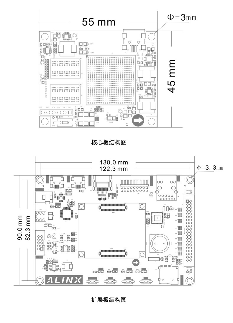
130mm x 90mm
Number of layers
4-layer PCB with reserved independent GND layer

The monocular camera module AN5640 collects video and displays it on the monitor through the VGA interface of the development board


Single camera and AN430 LCD screen module display diagram
AN9767/AN706 module on machine display diagram

*The signal output from the signal source is connected to the AN9767 module and the waveform signal is displayed through an oscilloscope
*The signal output from the signal source is connected to the AN706 module, and the system is run to draw waveform data, which is displayed on the display through the VGA interface of the development board
The warranty period of all products sold is 12 months, of which FPGA chips and LCD screens are wearing parts and are not covered by the warranty. All accessories and gifts are not covered under warranty.